
MITRE STEM Outreach
MITRE’s STEM Outreach team is inspiring the next generation of leaders and innovators to pursue careers in STEM and join us in solving problems for a safer world.
Who We Are
MITRE’s STEM Outreach team is a Business Resource Group composed of volunteer leaders leveraging the expertise of MITRE’s employees to build the future STEM talent pipeline. We engage with educators, parents and students across the country to offer large-scale and local engagements, virtual workshops, and self-service resources.
Latest News
MITRE STEM: Growing the Future Microelectronics Workforce
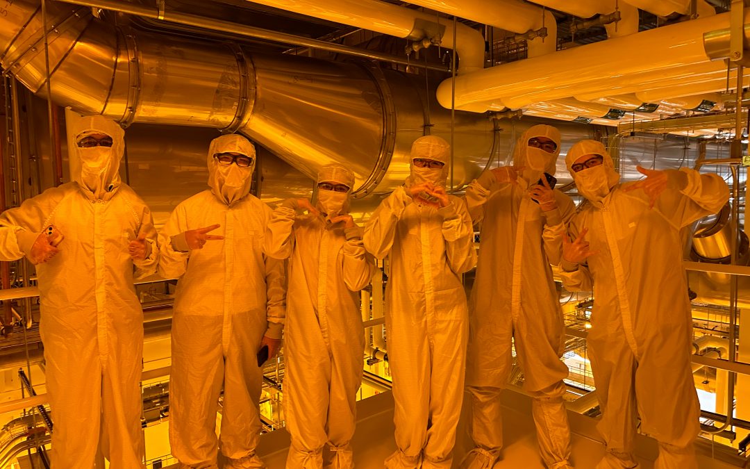
On a brisk January day, MIT.nano transformed into a hub of youthful curiosity and innovation, hosting a unique workshop in partnership with MITRE’s Basics of ASICs (the acronym means “application-specific integrated circuit”) class taught at MIT’s Beaverworks Summer Institute. This event welcomed six high school students from Massachusetts, New York, and Florida, offering them accelerated access into the amazingly complex world of semiconductor manufacturing. It was a day dedicated to demystifying some of the processes behind chip making, specifically focusing on lithography while providing the students with a rare hands-on learning experience.
Guided by Dr. Jorg Scholvin, assistant director of user services at MIT.nano and supported by a diverse team from MITRE including Mike McGivern, Melvin Lin, and Dr. Shelby Savage, the workshop kicked off with a compelling introduction to the nano-world’s astonishing properties. Dr. Scholvin’s discussion on cleanroom safety and etiquette prepared the students for a day filled with discovery and hands-on application.
Learning Mastery of Small Details
The participants embarked on a detailed exploration of the chip-making process, from wafer preparation to photoresist application, lasing, chemical etching, and die separation. Their efforts resulted in the creation of two 8” wafers and a personal 5” wafer with each student’s photos as a souvenir marking their achievement and potential futures in this discipline.
Reflecting on the workshop’s impact, one student shared their newfound understanding.
“I learned about the precision needed to work with silicon wafers” they say. “When we looked under the microscope to see the etched image and check for any flaws or misalignment, I realized the unbelievably tiny scale of our work and how crucial the smallest details were.” This realization underscored the workshop’s ability to not only impart technical knowledge but also to open students’ eyes to the meticulous nature of semiconductor manufacturing.
“The cleanroom was certainly very dry, but wearing the bunny suit made me feel like a real scientist,” comments one participant, highlighting the immersive and authentic nature of the experience. Another student, aspiring to a career in computer engineering, found the workshop particularly enlightening, “Seeing the processes that I might potentially employ in my future studies or career is incredibly eye-opening.”
The workshop was more than a lesson in technical skills; it was an opportunity for students to envision their future in science, technology, engineering, and mathematics (STEM) fields. Asked about whether the visit broadened their horizons on careers one student replied, “Yes! Although I haven’t narrowed down to a specific field the MIT.nano visit introduced a new field of interest that I will continue to investigate in the future.”
The workshop not only offered a glimpse into the future of technology but also created an additional touchpoint for collaboration between MITRE and MIT.nano.
“This is such an exciting and important point in time for microelectronics—not just for creating new innovations in the field, but also for educating and inspiring the next generation of scientists and engineers that will transform it into the future,” says Dan Walters, who leads MITRE’s microelectronics horizon strategy. “MIT.nano is an amazing facility that is complementary to MITRE’s own in-house microelectronics capabilities, and so I’m very excited to collaborate with MIT on workforce development and other important initiatives.”
The significance of the workshop extended beyond the day’s learning activities. A wafer crafted during the workshop was presented to the Massachusetts Gov. Maura Healy and Dr. Dev Shenoy (principal director of the Office of the Undersecretary of Defense for Research and Engineering) at the New England Microelectronic Commons (NEMC) event. MITRE received a special acknowledgment for our role in mentoring the students and helping to create this opportunity for high school students.
About the MITRE STEM Council
This workshop is one of many organized and hosted with support from the STEM Council, a MITRE Business Resource Group composed of volunteer leaders leveraging the expertise of MITRE’s employees to build the future STEM talent pipeline. We engage with educators, parents, and students across the country to offer large-scale and local engagements, virtual workshops, and self-service resources. The STEM Council is always open to volunteers and partnership opportunities.
Visit STEM.mitre.org to learn more and join the MITRE STEM mailing list.
—by Mike McGivern
©2024 The MITRE Corporation. ALL RIGHTS RESERVED.
Approved for Public Release; Distribution Unlimited. Public Release Case Number 24-0760